Section 1.2: Transistors #
Every transistor makes a demand on the stage that drives it. A bipolar junction transistor (BJT) asks for current: a small base current controls a larger current between collector and emitter. A field-effect transistor (FET) asks for voltage: the gate voltage controls current through a channel between source and drain. Both use the same doped semiconductor as a diode, so much of their behavior follows from the previous section.
Current Control in a BJT #
A BJT’s base and emitter meet at a PN junction, and base current flows only when that junction is forward biased. In an NPN transistor, the base is the P-type layer, so forward bias means making the base positive relative to the emitter. The junction behaves like the silicon diode it is: current rises sharply once the voltage nears the forward threshold.
That base current controls a much larger collector current. The transistor’s current gain, called beta and written , measures that control. The higher the beta, the less base current the driving stage must supply for a given change in collector current.
For example, if a 0.1 mA change in base current produces a 10 mA collector-current change, divide 10 by 0.1 to find the current gain: . The extra output energy comes from the collector supply; the base current only decides how much of it flows.
Key Information:
- A silicon NPN transistor biased on has a base-to-emitter voltage of approximately 0.6 to 0.7 volts.
- The beta of a BJT is the change in collector current with respect to the change in base current.
Gain at Higher Frequencies #
That gain doesn’t hold at every frequency. Charge takes time to move through the device and to fill and empty its junctions. At high enough frequencies, the signal changes faster than the transistor can follow, and current gain falls.
A cutoff frequency marks where gain has fallen by a set amount, and which gain you measure depends on which terminal the input and output share. With the input at the base and the output at the collector, the two share the emitter, so beta is the common-emitter gain. Alpha compares collector current with emitter current. The base is then the shared, or grounded, terminal, so alpha is the grounded-base, or common-base, current gain. Because emitter current is collector current plus base current, alpha always falls just short of 1. Beta has a cutoff frequency of its own, measured on common-emitter gain.
Key Information: The alpha cutoff frequency is the frequency at which the grounded-base current gain of a bipolar junction transistor has decreased to 0.7 of the gain obtainable at 1 kHz.
Controlling the Channel #
When base current would load the driving stage too heavily, an FET offers another approach. Its gate draws almost no steady current.
A junction FET, or JFET, controls the channel through a reverse-biased junction, which passes only a tiny leakage current. A MOSFET uses a gate insulated from the channel by a very thin layer; its name expands to metal-oxide-semiconductor FET.
Key Information: The DC input impedance at an FET gate is higher than that of a bipolar transistor.
That holds for DC. A changing signal still draws current to charge and discharge the gate’s capacitance, so the stage driving a transmitter’s power MOSFET has real work to do.
Before biasing an FET, you need to know whether its channel conducts with no gate voltage. Some FETs come with the channel already in place. Gate bias can deplete that channel of carriers and reduce its current, which gives this type its name.
Key Information: A depletion-mode FET is an FET that exhibits a current flow between source and drain when no gate voltage is applied.
An enhancement-mode FET works the other way: its channel needs suitable gate bias to conduct strongly.
Recognizing the Symbols #
An FET symbol shows how its gate is built. A gap between the gate line and the channel indicates an insulated gate; a gate line that touches the channel marks a JFET. Two separately labeled gates identify a dual-gate device, which accepts two control signals on the same channel. The arrow shows the channel type. As in a diode symbol, it points from P toward N: into an N-channel device, out of a P-channel one.
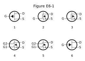
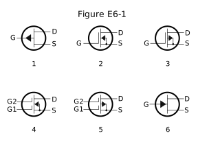
In symbol 1, the gate touches the channel and the arrow points out. Symbol 4 has two insulated gates and an arrow pointing in.
Key Information:
- Symbol 4 in Figure E6-1 is an N-channel dual-gate MOSFET.
- Symbol 1 in Figure E6-1 is a P-channel junction FET.
Protecting the Gate #
The thin insulation that gives a MOSFET its high input impedance is also easy to damage. Excessive voltage can puncture it. Because the gate’s capacitance is small, even a little static charge can raise its voltage that far despite carrying little energy. A spark you can feel takes a few thousand volts; one too small to notice can still do the job.
The Zener diode can help here. Its breakdown voltage sits above the normal gate voltage but below the level that would harm the insulation, so it doesn’t conduct during normal operation. If static pushes the gate voltage higher, the Zener conducts and limits the voltage before the insulation breaks down.
Key Information: Zener diodes connected between a MOSFET gate and its source or drain protect the gate from static damage.
Not every MOSFET has that protection built in, so touch something grounded before you handle one.




 Base-to-emitter voltage of approximately 0.6 volts to 0.7 volts