Section 1.1: Diodes and Junctions #
You probably know the diode best as a one-way valve for current, the part that lets a power supply’s rectifier turn AC into DC. An LED is a diode too; it gives off light while it conducts.
That sells the diode short. With the right design, a diode can hold a voltage steady, pull the audio out of a radio signal, tune a receiver, or steer a signal from one path to another. To get those jobs out of it, you need a look inside, starting with the two kinds of material a diode is made from.
Two Kinds of Semiconductor #
In most diodes, both kinds of material start out as silicon, a semiconductor. Pure silicon is a poor conductor, because nearly all its electrons are locked into bonds with their neighbors. Manufacturers change that by adding a pinch of other elements, a process called doping. The added atoms change the supply of movable charges, or charge carriers, and they can do it in two different ways.
Some added atoms, called donors, each bring an extra electron that is free to move through the crystal and carry current. Others take electrons from neighboring bonds. A hole is the gap where a bond is missing an electron. When a nearby electron fills it, that electron leaves another hole behind. Picture an empty seat in a crowded row: as each person slides over to fill it, the empty seat travels the other way. The hole moves opposite to the electrons, so it behaves as a positive charge carrier.
Key Information:
- N-type semiconductor material contains excess free electrons.
- An impurity atom that adds holes to a semiconductor crystal structure is called an acceptor impurity.
Electrons are the majority carriers in N-type material; holes are the majority carriers in P-type material, the kind acceptors produce. On its own, either material conducts in both directions. The one-way behavior appears only where the two meet.
Where P Meets N #
Form P-type and N-type regions side by side in one crystal, and their boundary becomes a PN junction. Near the boundary, electrons and holes spread into the opposite material. When an electron fills a hole, neither remains available as a mobile carrier. This is recombination. It leaves a narrow depletion region with few mobile charges. Each donor that gave up its electron becomes positively charged, and each acceptor that took one becomes negative. These charged atoms stay fixed in the crystal. Without the mobile charges to balance them, they create an electric field. That field acts as a barrier, a hill that carriers must climb to cross the junction.
Applying a steady voltage can change that barrier and set the diode’s operating condition; this is called biasing. The P side is the anode, and the N side is the cathode.
With forward bias, the anode is positive relative to the cathode. The applied voltage pushes carriers toward the junction and lowers the barrier. A small forward voltage lets only a trickle of current across. Near the forward threshold voltage, about 0.7 V for silicon, current begins to rise sharply, and the rest of the circuit must limit how much flows. While the diode conducts, the voltage across it, its forward voltage drop, stays near that threshold and rises only slowly as the current increases.
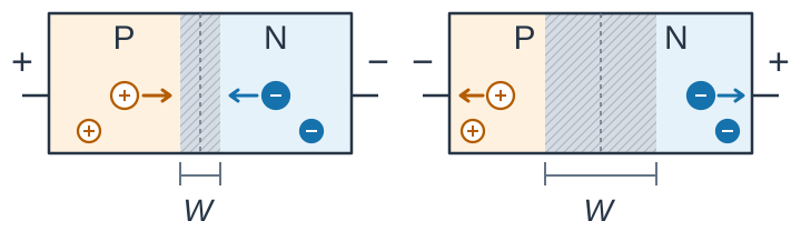
Reverse bias makes the anode negative relative to the cathode, reversing the push that forward bias gives the carriers.
Key Information: A PN-junction diode does not conduct current when reverse biased because holes in the P-type material and electrons in the N-type material are separated by the applied voltage, widening the depletion region.
Only a small leakage current gets through.
Nearly everything a diode does comes down to that barrier and which way you push it. Diodes that rectify, detect, or give off light work with the barrier lowered. Diodes that hold a voltage steady or tune a circuit put reverse bias to work. Others change how the junction itself is built. Forward conduction comes first, since every rectifier depends on it.
The Cost of Conducting #
Nothing crosses the junction for free. The forward voltage drop shows how much energy each bit of charge gives up, and diode loss is that drop multiplied by the current. At 1 A, a 0.7 V drop dissipates 0.7 W.
In an ordinary silicon diode, that energy becomes heat right at the junction. Some heating is normal, as long as the package can shed heat as fast as the junction makes it. Push too much current through, and the heat builds faster than it can escape.
Key Information: Excessive junction temperature causes a junction diode to fail from excessive current.
Light Instead of Heat #
The energy a diode gives up is released when electrons and holes recombine, and it doesn’t have to come out as heat. Electrons in a semiconductor occupy ranges of energy called bands. In the valence band, electrons take part in bonds; in the conduction band, they can move through the material. The band gap is the energy difference between those ranges. Moving up across it requires energy; moving down releases energy. When an electron that has crossed the junction falls into a hole, it drops across the gap and gives up that energy.
In silicon, nearly all of it becomes heat. An LED uses materials that release much of it as light instead, in packets called photons. The size of the band gap sets how much energy each photon carries, and that determines the light’s color. The applied voltage has to give each carrier that much energy. Blue light carries more energy per photon than red, so a blue LED needs roughly 3 V, compared with about 2 V for red.
Key Information: The band gap of an LED’s semiconductor material determines its forward voltage drop.
A Lower-Loss Junction #
Because the band gap sets the forward voltage, choosing a different semiconductor is one way to lower the drop. Changing the junction itself is another. Joining a metal directly to a semiconductor, instead of joining P-type and N-type material, also forms a barrier, but a lower one, so the forward drop falls to about 0.3 V. In a rectifier carrying 1 A, that wastes 0.3 W instead of a silicon diode’s 0.7 W. At 20 A, the difference is 8 W less heat in every diode the current passes through, and more voltage left for the load.
Key Information:
- A Schottky barrier diode is a metal-semiconductor junction.
- A Schottky diode’s lower forward voltage drop makes it a better choice than a silicon junction diode for use as a power supply rectifier.
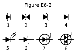
On a schematic, the diode types share the same triangle and bar, so the small marks on or near the cathode bar give each one away. In Figure E6-2, the ordinary diode (symbol 4) has a straight bar, the LED (5) adds light arrows, and the Zener (3) has angled ends on its bar. A Schottky’s bar has small squared hooks at both ends.
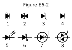
Key Information: Symbol 6 in Figure E6-2 is a Schottky diode.
Keeping Up with RF #
Forward conduction also lets a diode work as a detector. It rectifies an RF signal, producing a voltage that rises and falls with the signal’s strength. That voltage can recover the information the signal carries or show how strong the signal is. At VHF, the diode has to keep up with a signal that completes more than 30 million cycles a second.
The Schottky junction helps here, too. It stores very little charge, so it can switch quickly, and a small one has little capacitance to let the signal slip past. The same traits suit it to a mixer, which combines signals to produce new frequencies, as we will examine in Chapter 4. A point-contact diode, made with a fine wire touching a semiconductor, keeps its capacitance low another way: its contact area is tiny.
Key Information:
- Schottky diodes are commonly used as VHF/UHF mixers or detectors.
- A common use for point-contact diodes is as an RF detector.
Holding a Reference Voltage #
Now turn the junction around. Under reverse bias, an ordinary diode blocks current, but only up to a point. Raise the reverse voltage far enough and the junction reaches breakdown, where current can increase greatly. For an ordinary diode, breakdown is trouble, so designers pick one with enough reverse-voltage rating to stay well clear of it. A Zener diode lives there by design.
In breakdown, current climbs steeply for a tiny increase in voltage, much like the sharp rise at the forward threshold. That suits the Zener to its usual job as a voltage reference. A series resistor or other current-limiting circuit keeps it from overheating.
Key Information: The most useful characteristic of a Zener diode is a constant voltage drop under conditions of varying current.
Tuning with Voltage #
Below breakdown, a reverse-biased junction has another use. A tuned circuit’s resonant frequency depends on its capacitance, and older radios set it with a variable capacitor, a stack of metal plates turned by the dial. If a voltage could set that capacitance instead, a receiver could tune with no moving parts at all.
A reverse-biased junction already acts as a small capacitor. The depletion region separates its conducting P and N regions, much as an insulator separates a capacitor’s two plates. Charge can build up on either side even while the junction blocks DC current. More reverse bias widens the depletion region, as the right side of the junction figure shows. Wider separation means less capacitance.
Key Information: A varactor diode is designed for use as a voltage-controlled capacitor.
Switching an RF Path #
A diode can also switch an RF signal. Forward bias lets the signal through, and removing the bias blocks it, with no moving contact. Blocking is where the capacitance that was so handy for tuning becomes a nuisance. Even when a diode stops DC, RF can still sneak through that capacitance.
A PIN diode keeps that capacitance small. A nearly intrinsic, or undoped, layer between its P and N regions holds them farther apart than in an ordinary junction, so little RF leaks through when the switch is off.
Forward bias fills the intrinsic layer with charge carriers, and the more current flows, the more easily RF passes. A current between full on and full off leaves the diode partly conducting, so it can reduce a signal’s strength by any amount in between.
Key Information:
- Low junction capacitance makes a PIN diode useful as an RF switch.
- Forward DC bias current controls a PIN diode’s attenuation of RF signals.
A small DC current controlling an RF signal is a neat trick. A transistor takes the idea much further, letting a small current or voltage control a much larger one.



 N-type